Strategic Partnership with AWS Marks a Key Step in ST’s Photonics Expansion
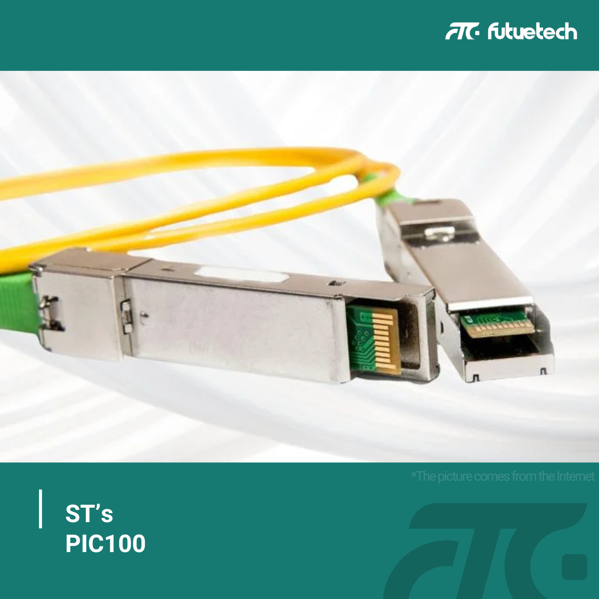
Global semiconductor supplier STMicroelectronics (ST) has officially entered the silicon photonics market with the launch of its first silicon photonic integrated circuit (PIC) platform, PIC100. This solution is designed to optimize optical interconnect performance in data centers and artificial intelligence (AI) infrastructure. By integrating silicon photonics (SiPho) with BiCMOS technology, the PIC100 platform offers high bandwidth, low power consumption, and extended transmission distances, making it ideal for next-generation optical modules and transceivers. ST has partnered closely with Amazon Web Services (AWS) to drive the commercialization of silicon photonics technology.
Silicon Photonics + BiCMOS: A High-Performance Optical Interconnect Solution
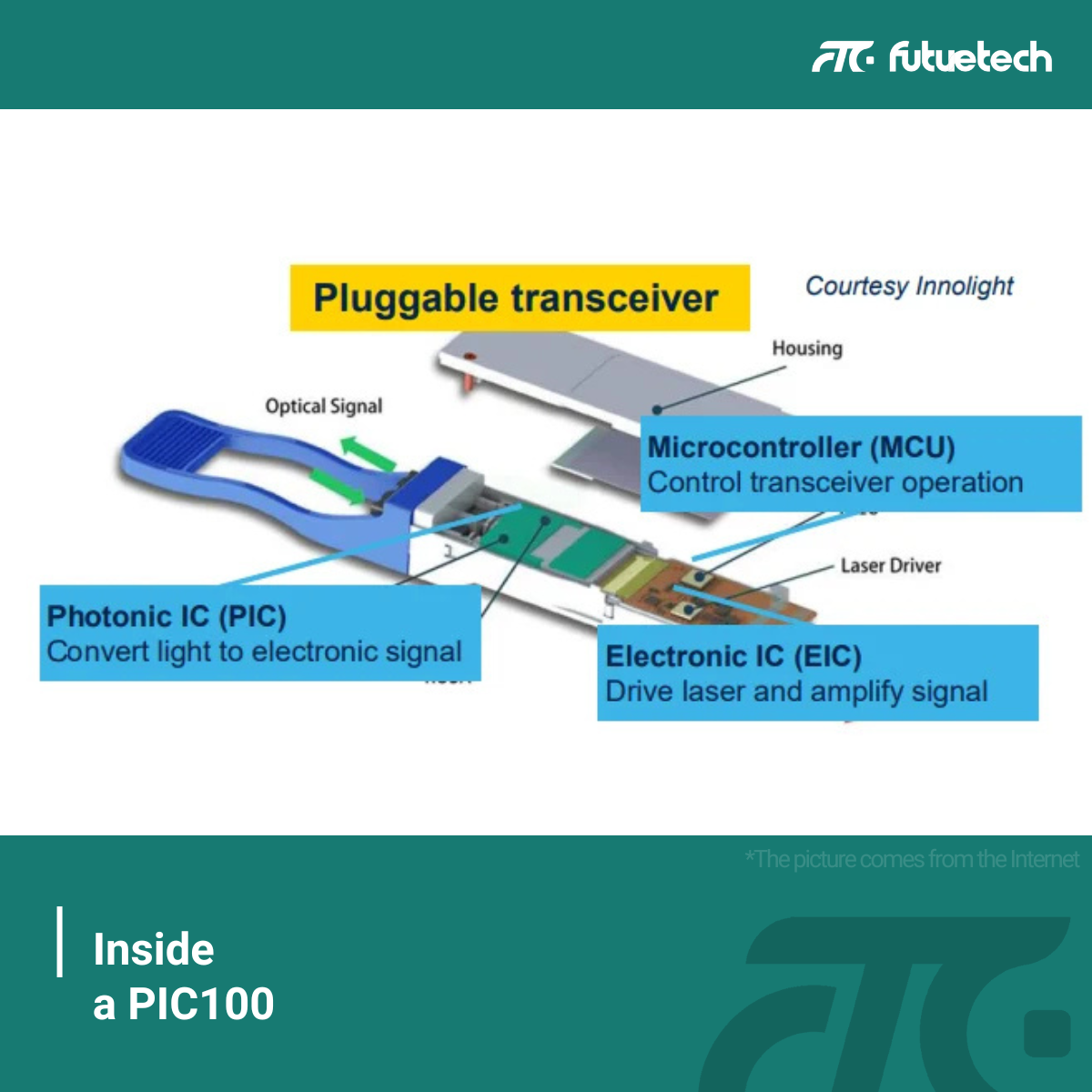
The PIC100 platform is a 300-mm silicon photonics solution that leverages ST’s expertise in BiCMOS technology to enable highly efficient electro-optical signal conversion. Unlike traditional electro-absorption modulated laser (EML) and vertical-cavity surface-emitting laser (VCSEL) solutions, PIC100 is built on a pure silicon platform, achieving 200 Gbps per lane. This provides a scalable and efficient alternative for the optical communications industry.
“PIC100 is currently the only 300-mm silicon platform capable of supporting up to 200 Gbps per lane, equivalent to 100 Gbps in PAM4 modulation, which is how it got its name,” explained Vincent Fraisse, General Manager of STMicroelectronics’ RF and Communications Division.
ST’s BiCMOS B55X process plays a crucial role in optimizing signal processing for silicon photonic circuits. This process offers outstanding linearity, high-frequency performance, and low-noise amplification, supporting high-speed transimpedance amplifiers (TIAs) and laser drivers to ensure signal integrity, even at 200 Gbps per lane. Additionally, the BiCMOS B55X process is particularly well-suited for linear pluggable optics (LPO) and linear receiver optics (LRO), eliminating the need for DSP-based equalization and further reducing power consumption and latency.
Advanced Manufacturing and Scalable Mass Production
The PIC100 platform is manufactured using 300-mm wafer technology, ensuring greater process uniformity and higher yield rates for cost-effective large-scale production. ST’s Crolles, France, facility employs advanced immersion lithography to deliver industry-leading process consistency and digital-CMOS-class yield performance.
PIC100 integrates high-density silicon photonic components, including modulators, photodetectors, and waveguides, improving system efficiency while reducing component complexity. Furthermore, the platform adopts an innovative edge coupler for fiber attachment instead of traditional grating couplers. While grating couplers simplify alignment during testing, they introduce significant optical losses due to mode mismatch and scattering effects. ST’s edge coupler design achieves coupling losses of less than 1.5 dB, enhancing link efficiency and extending transmission distances.
“With an innovative material stack-up, PIC100 enables direct fiber attachment at the edge of the photonic IC, significantly reducing system losses—one of the key challenges faced by transceiver developers,” Fraisse added.
Silicon Photonics Driving Data Center Interconnect Evolution
As hyperscale data centers and optical module manufacturers increasingly adopt silicon photonics, ST is actively expanding its roadmap to meet growing market demands. AWS has been a key development partner in the PIC100 project and plans to deploy the technology in its infrastructure once it reaches production readiness.
“AWS has signed a collaboration agreement with ST, playing a deep role in PIC100’s development and will integrate this technology into its data centers once it enters mass production,” Fraisse confirmed.
Looking ahead, ST aims to further enhance its silicon photonics product line. Future versions will support 400 Gbps per lane and incorporate advanced electronic components, such as germanium-silicon photodetectors (GeSi PD) and hybrid III-V semiconductor lasers, to improve overall efficiency and system performance. Additionally, ST plans to introduce through-silicon via (TSV) integrated optical interconnects to enable direct chip-to-chip optical communication, reducing PCB traces and copper interconnects to enhance data transmission density and speed in AI accelerators and compute clusters.
ST targets mass production in the second half of 2025. With continuous advancements in silicon photonics technology, STMicroelectronics is committed to driving the evolution of optical interconnects for hyperscale data centers and AI computing infrastructures, spearheading the transformation of next-generation optical communication.